
Due to the human pursuit of the ultra-high-definition display, the pixel pitch of LED displays is constantly shrinking. As the first generation of display technology, the traditional SMD display has been very mature after more than ten years of development. With the development of LED display technology, technical routes such as COB and IMD have come out. Also, different packaging routes can be matched with different chip structures. So, which technical route will finally aspire to in the era of micro-display?
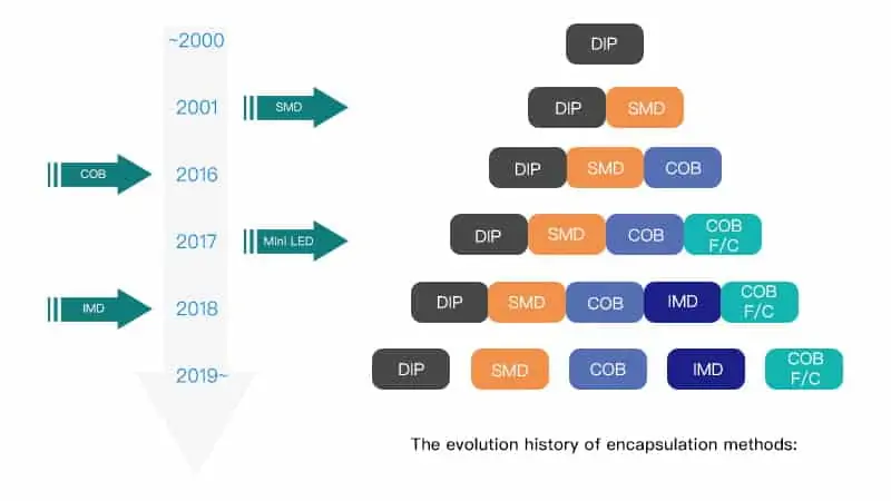
The evolution history of encapsulation methods:
LED display encapsulation, from DIP at the beginning of the industry, has now developed into an industrial pattern in which multiple packaging methods such as DIP, SMD, IMD, and COB coexist.
What is COB?
COB, is the abbreviation of Chips on Board in English. It is a method of circuit board manufacturing in which the integrated circuits (e.g. microprocessors) are wired, bonded directly to a printed circuit board, and covered by a blob of epoxy glue. Because the bare chip is directly exposed to the air, it is easy to be polluted or artificially damaged, which affects or destroys the function of the chip, so the chip and the bonding wires are sealed with glue and simplifying the packaging structure of ultra-fine electronic components and improving the stability of the final product.
In the process of developing towards the MicroLED era, it is difficult for SMD encapsulation to break through the narrower pixel pitch, and it is difficult to ensure high reliability and protection. For this purpose, the industry needs the relay of technical routes such as COB.
Features of COB
1. With ultra-high reliability
COB technology eliminates the process flow of SMD light-emitting tube packaging, color separation, taping, and patching, shortens the process path, and improves the reliability of the product production process. The COB product panel is potted as a whole, which is moisture-resistant, anti-collision, and has a protection level of IP65. There are no exposed pins and anti-static breakdown, which improves the reliability and stability of the display.
2. COB package is suitable for products with the small pixel pitch
The COB technology route is not limited by the physical size, bracket, and lead of the SMD LED package, and can break through the SMD pitch limit, achieve higher pixel density, and have a more flexible dot pitch design.
3. COB realizes the conversion from “point” light source to “surface” light source
No pixel graininess; can effectively control the brightness of the pixel center, reduce the intensity of light radiation, inhibit moiré, glare and glare to the retina, suitable for close and long-term viewing, not easy to cause visual fatigue, suitable for close-screen viewing.
4. Truly fully sealed structure
The PCB circuit board, crystal particles, solder feet and leads are fully sealed. The advantages of the sealed structure are an obvious-for example, moisture resistance, anti-collision, prevention of pollution damage, and easier cleaning of the device surface.
COB encapsulation technology has obvious advantages such as high reliability, high assembly efficiency of the entire screen, and soft light output from surface light sources. It can be applied to any pitch of millimeters in theory, but the materials required are expensive. Also, to solve the consistency of display and appearance, the problem requires a higher cost.
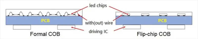
NOW, COB Flip-chip is the future of display
As an upgraded product of formal COB, flip-chip COB is based on the advantages of formal COB ultra-small dot pitch, high reliability, and non-glaring surface light source. Further, improve the reliability, simplify the production process, better display effect, perfect near-screen experience, and real chip-level spacing can be realized.
What is the difference between a traditional COB chip and a COB flip-chip?
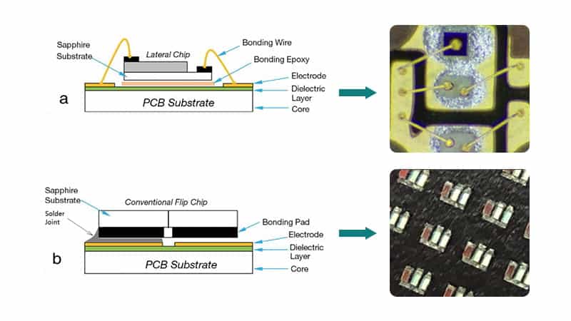
1. Only Flip-Chip COB can achieve true chip-level spacing, reaching the level of Micro LED. This is because, from the perspective of the LED chip, the Flip-Chip does not require wire bonding, which breaks the pixel pitch limit of the formal chip and solves the problem of metal migration in the formal LED.
2. Also, each pixel unit has 6 metal bonding surfaces, which effectively solves the problem of poor wire breakage due to dashed wire bonding, and further improves reliability. From the perspective of encapsulation, Flip-Chip COB encapsulation is a true chip-level integrated encapsulation, wireless bonding, and the physical space size is only limited by the size of the light-emitting chip, which can achieve higher pixel density.
3. In terms of display performance, the area of the Flip-Chip is smaller on the PCB board, and the duty cycle of the substrate is increased. It has a larger light-emitting area, which can present a darker black field, higher brightness, and higher contrast.
4. Presents HDR-level display effects. Moreover, there is no welding wire link, which effectively simplifies the production process and reduces the equipment investment cost. As the industry scales, the product cost will be greatly reduced, especially when the dot pitch is less than 1.0mm, it will have a cost-competitive advantage.
Therefore, Flip-Chip COB technology is a necessary condition for the realization of MicroLED and will go further in the era of micro-display.
Thanks to the development of small-pitch LEDs, COB, IMD, SMD, and other technologies have been prosperous in recent years, and step by step to the forefront of the world. In particular, COB technology differentiates between formal-chip and flip-chip, the Flip-Chip does not require a wire bonding process, and in conjunction with the integrated encapsulation COB and IMD, the pixel pitch can be effectively narrowed, and the chip size is further miniaturized, and it is believed that flip-chip COB is the future of display!